Scanning Tunneling Microscopy of 1D and 2D Materials
Scanning tunneling microscopy (STM) is a technique that enables atomic resolution imaging of conducting and semiconducting surfaces. Together with scanning tunneling spectroscopy (STS), STM is used to image and measure the electronic properties of surfaces, molecules, and nanomaterials. The Lyding group investigates a wide variety of 1D and 2D materials including graphene, graphene nanoribbons, and carbon nanotubes. STS is used to obtain detailed electronic information which is essential when evaluating candidates for high-performance electronic devices. the role is surface and any adsorbed molecules are sensed by a tunneling current — making investigation of surface physics on atomic-scale possible.
With increasingly demanding miniaturization and performance requirements in the electronics industry, atomically precise graphene materials may play a significant role in high-performance computing. A previous scanning tunneling spectroscopy study published by the Lyding group in Nature Materials experimentally determined that structural details at the atomic scale have a large effect on the electronic properties of graphene nanostructures. As a result, atomic precision is required to obtain well-controlled electronic properties. Through the bottom-up approach, nanoribbons can be made with atomic precision, enabling control over their electronic structure.
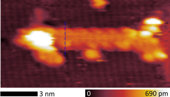
Graphene nanoribbons are synthesized either on metal surfaces using molecular precursors, or synthesized in solution as demonstrated by the Sinitskii group, our collaborators at the University of Nebraska-Lincoln. Previously, several groups have shown that nanoribbons can be transferred from the metal substrates onto other substrates using wet chemical methods, but high-quality images and electronic measurements could not be obtained due to problems associated with solvent residue. Our work, published in Nano Letters (DOI: 10.1021/acs.nanolett.6b03709), shows that solution-synthesized graphene nanoribbons can be cleanly placed onto arbitrary surfaces using the dry contact transfer method.
We use optically assisted STM to study absorption and intermolecular energy transfer between single quantum dots (QDs) and carbon nanotubes (CNTs). Single PbS, CdSe, CdSe/ZnS, CdSSe/ZnS QDs and CNTs are deposited onto gold, crystalline silicon carbide (c-SiC) and a-SiC surfaces by matrix-assisted dry contact transfer. Adsorbed molecules are excited with modulated laser light and the modulated tunneling current proportional to the optical absorption signal is detected by STM with a lock-in amplifier.